Matt’s back in town! (with pictures of black silicon…)


I’m back in Richmond now, having just returned from a year-long research sabbatical in France working on a new project involving “Black Silicon.” When a smooth surface of pure silicon is subjected to plasma etching under certain special conditions, it can spontaneously form a dense forest of microscopic spikes and holes, typically a few hundred nanometers across and a handful of microns high.  As a result of this extreme roughness, light which is incident on the surface becomes trapped, and is eventually absorbed by the material, making it appear black to the naked eye.  Beyond the many interesting physics questions this material raises (How does this happen?  What determines the length scale?) this material has several potential applications, including the possibility for more efficient solar cells.

A scanning electron microscope image of black silicon

My work in France was at ESIEE Paris, an engineering school in the eastern suburbs of Paris.  I will continue to work on this project here at Richmond, collaborating with my French colleagues remotely.   Although we don’t have the plasma etching equipment here, we do have access to microscopy and analysis tools.   I also expect to return to Paris for several weeks at a time during the summers.

The LHC: the world’s purest diamond and my 50 micron contribution to a 17 mile tunnel

With the recent news of the successful startup of the large hadron collider (LHC) at CERN, I’m reminded that I actually worked on a small piece of it back in the late 1990s, in one of my former lives as a graduate student at Ohio State University.  The LHC is the new, big, expensive, high energy particle accelerator, a 17 mile long tunnel that will accelerate particles to very high speeds, ultimately making collisions which will  mimic the conditions of the early universe just after the big bang. 

My own tiny piece of the project involved making tracking devices to detect the particles ejected from these high energy collisions. These tracking devices consist of a thin slab of insulating or semiconducting material, with a grid of tiny metal wires running horizontally on one side and vertically on the other.  When a high energy particle comes tearing through, it ionizes atoms in the material, creating small voltages on the nearby wires.  By monitoring the voltages on all of the wires, scientists can measure the precise x-y location of the high energy particle.  The actual detector at the end of the 17 mile long tunnel consists of many thousands of these devices, arranged in a sphere surrounding the area where the collision occurs.  By accurately tracking all of the particles ejected from a collision, scientists can work backwards to understand the physics of the collision itself.

In an accelerator as powerful as the large hadron collider, the spray of ejected particles would basically shred ordinary tracking devices, which are normally made of silicon.  I worked briefly with the RD42 collaboration to help develop tracking devices made of diamond, which is much less susceptible to radiation damage.  As part of the project, the group helped develop very high purity synthetic diamonds made by a chemical vapor deposition (CVD) technique.  The chemical and electrical purity of these diamonds easily surpasses that of any naturally occurring diamond on the earth, and at one point I actually held in my hand what at the time was the most perfect diamond the world had ever seen.  (It looked like a small piece of glass, about a centimeter square, maybe a couple of millimeters thick.) 

I helped the group to perform the lithography required to pattern the diamond’s surfaces with a dense array of 50 micron gold wires, about the thickness of a human hair.  (It was a fairly standard application of existing lithography technology, made only slightly trickier by the roughness and optical properties of the diamond surface.)  Interestingly, I never set out to be a high energy physicist, and initially I didn’t have anything to do with the group working on the LHC at Ohio State University.  At the time, I was actually using lithography to attach electrodes to tiny superconducting crystals for a completely unrelated experiment; I just happened to be the local expert there when the LHC group needed some help to prepare for some upcoming “beam time” at another accelerator.  I took time away from my normal Ph.D. work to help them out, and it ended up being a very interesting and ultimately successful collaboration.

The moral of the story, for those of you who like that sort of thing, is to pay attention to what your colleagues are working on, even if it seems unrelated to what you’re doing.  There may be connections to your own work that aren’t so obvious.  The LHC is a huge project, and many thousands of people have contributed to it; I sometimes wonder how many of those are accidental contributors like me.  Accidental or not, I’m proud to have played even a tiny technical part in the experiment, and I look forward to the new physics it will tell us.

What is Undergraduate Research, Anyway?

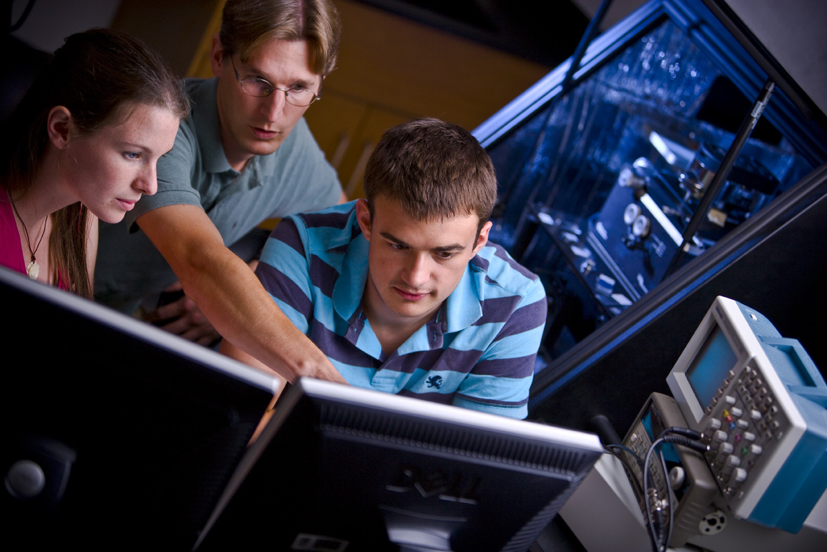
I’ve gotten several questions recently from prospective students and their parents asking how undergraduate research works.  Who does it?  When does it start?  What do they do?  What is undergraduate research, anyway?

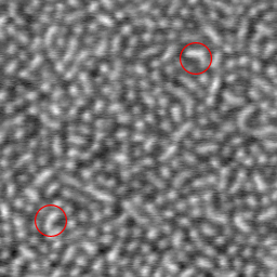
As a professor, I have two jobs.  One is to teach students, as I do every day in my classes.  The other is to do research, which in my case involves doing experiments, taking data, figuring things out, and then presenting it at conferences and in articles in scientific journals.  At big universities like Ohio State and Princeton (where I was before), research is done in groups involving at least one professor plus a small army of post-docs and graduate students.  At Richmond, we do the same thing but with undergraduates.  We study the same kinds of problems, present at the same national and international conferences, and publish in the same journals.  (Does size and lack of graduate students put us at a disadvantage?  Only a little bit.  Some projects require millions of dollars and dozens of graduate students; other projects don’t.  I have to be a little bit careful picking my projects, but there are plenty of unanswered questions out there that I can find the answers to just fine here, thanks.  In fact, most of us collaborate with colleagues from other schools, too.)

In our physics department, all six of the tenure-line faculty are research active.  (That’s not true at all small colleges, where it’s common for some of the faculty, particularly senior professors who were hired under different expectations, to support their school’s mission in other ways.  Some other colleges may also lack the resources to support research at the level we do.)  If each of us works with three or four students, the total number of physics students involved in undergraduate research is…well, pretty much all of them, including students only in their first or second year.  Note that in our department, research is not just for seniors doing “senior projects” or for only the top honors students.  Students typically do research during the year for course credit, and most do research over the summers for money, paid by the University or from a professor’s research grant.

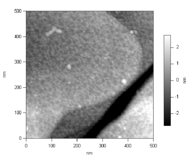
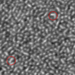
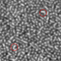
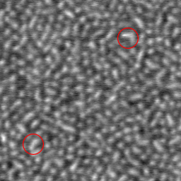
Students here do research on whatever topics the faculty are studying.  For me, that means copolymer materials, nanotechnology, and atomic force microscopy.  (Other professors here study nuclear physics, particle physics, biological physics, and cosmology.)  Although in principle a student could pursue a topic independently, in practice that never happens, simply because figuring out what problems are truly new and interesting (and practical) at the forefront of human knowledge is virtually impossible for a novice.   (And if it’s not at the forefront of human knowledge, we’re not generally interested in it here at UR.  Topics like “the physics of skiing” are fun and might even be a good learning experience, but that’s just not what we do.)  There is no formal process for matching students with faculty; by their sophomore years at the latest, our students generally recognize the benefits of doing research and tend to be drawn to one professor’s lab or another.  The professors are always on the lookout for new students too, and in a department as small and informal as ours, connections just happen.

Doing research is a great experience for our students.   They are often authors on journal articles, and they get to travel to national and international conferences to present their work–all of which looks pretty good on a resume for graduate school or for jobs.  The skills they learn, both specific technical skills and a more general ability to tackle open-ended problems and deal with complexity,  are applicable wherever they go.  And for me, it’s great to see how students grow from their first tentative steps as incoming students, to confident and capable seniors who go on to do great things.  In this way, my two jobs–teaching and research–are really just one job, like two faces of the same coin.

So long, Nate!

This summer Trawick lab bids farewell to Nate Lawrence, who graduated in the spring but stayed on to continue working on his research project over this summer.  Nate starts graduate school in electrical engineering at Boston University this fall.

Nate is a great example of a student who took advantage of the opportunity to do research here.  He started working with me as a first year student, learning to use the atomic force microscope in our lab.  His research continued here over the summers, supported by a summer fellowship from the Virginia Foundation for Independent Colleges, and later by a grant from the Research Corporation.  Over the course of four years, he has become a highly skilled researcher and a real expert in the field, and his work was presented at several national physics conferences.  During his four years at UR, Nate spent one summer doing research at Boston University, and also spent a semester abroad in Scotland.  He won the Robert Edward Loving Award in Physics for promise for advanced study in physics.

Nate’s expertise will be sorely missed around here.  So long, Nate, and stay in touch!

Yee-ouch, them pins is pointy! (Our highest resolution microscope image ever)

Over the last few months, we’ve been collaborating with Mike Leopold and his students in the chemistry department to use our atomic force microscope to image their nanoparticle films.  We just purchased a small number of extra sharp (and extra expensive) tips for the microscope that allow us to resolve surface features about 1 nanometer in size.  This image of a thin gold film that was coated over a mica surface is our first picture with the new tips.  The mica is mostly very smooth, except for the big crevasse in the lower right hand corner.  The surface roughness that you see is from the gold film, which clumps together to form small “grains” about 20-30 atoms across, or about 10 nanometers.

baregold-0008.png

Take a moment to appreciate the scale of this picture.  The vertical scale at the right shows that the darkest areas are about 5 nanometers lower than the whitest areas; most of the surface roughness is on the order of about two nanometers.  The entire image is 500 nanometers across, or half a micron.  If it shows up on your computer screen as 4 inches across, then the width of a human hair on the same scale would be about fifty feet! 

This image was taken by my student, Nate Lawrence.

Matt needs more research students!

One of the nice things about teaching is seeing my students graduate and go on to do cool things elsewhere.  Of course, it’s not so nice when my entire lab group graduates all at once, as happened this spring!  (Nate…Jill…Brian…David!  Please come back!)

Anyway, I just want to put the word out there that I’m very actively looking for some students to join me in fall of 2008 and beyond.  I have a handful of projects I’ll be involved in; some projects will entail using the cool and expensive atomic force microscope in our lab; others will involve more computer coding and analysis.  I’m especially interested in finding a strong first or second year student.  I’m imagining working for course credit initially,  but I also have some grant money that could support a student over the summer.

One project I’ve written about here recently involves writing software to correct for distortion in atomic force microscope images.  This is a neat project involving a real-life application of numerical computing and image analysis; the resulting software package will be shared with potentially hundreds of scientists and engineers using around the world who use scanning probe microscopes.  Requirements: must be comfortable programming in C/C++, and must know some calculus.  (Everything else is learn-as-you-go.) 

Please contact me if you or anybody you know might be interested!

New results: distortion removed from AFM images

I thought I’d share a nifty result out of the lab that involves correcting distortion in the images we take with our atomic force microscope (AFM).

An AFM works by physically positioning a very sharp tip over a sample and rastering it back and forth over the image.  To look at nanometer-scale features as we do in our lab, this means having to physically position the tip over the surface with nanometer precision.  It turns out that even the best AFMs in the world run into a problem called thermal drift.  When the temperature in the room changes–by even a tenth of a degree–some parts of the microscope or the sample are always going to expand or contract with temperature by just a little bit more than other parts.  And that means that the tip can slowly move from where you thought it was.   Imagine scanning an image slowly–over several minutes–while the thing you’re imaging is moving under you.  The result is an image that can appear stretched, compressed, or badly skewed.

Check two pictures below, which are portions of two scans that were taken right after each other.   (One was scanned going up, the other scanned going down.)  The circled feature in the upper right is in the same place in each image, but the circled feature in the lower left is shifted slightly.  That’s because both images are slightly distorted from thermal drift.  On the left image, the distance between the two features appears to be is 400 nanometers.  On the right, it appears to be 357 nanometers.

complete_set_small2_i3.jpg   complete_set_small2_i4.jpg

Below are the same two images, after each one has been corrected using our new technique.  (They were corrected independently of each other; if all we did was use one as a guide for the other, that would be cheating!)  Now, in both corrected images, the features appear to be the same distance apart: 382 nanometers.

complete_set_small2_i1.jpg   complete_set_small2_i2.jpg

The way we corrected each image was by rescanning a small sliver from down the center of each image.  The rescanned sliver acts as a “key” to remove the distortion from the main image.  There’s actually a lot of computation involved in it, all performed by some numerically intensive computer software written by me and my student, Brian Salmons.

We still have a bit of testing and refining to do on our technique, but we hope we’ll have some published results soon.  (Watch for it in a journal near you!)  Of course, we’ll make our code available to the public.

 Later on, there are several features and enhancements I’d like to add, and I’m actively looking for a physics or computer science student at Richmond to work with.  If you’re interested in working on this project with me, let me know.

A nice picture of our microscope

Here are Jill, Nate, and me looking at some data on the our atomic force microscope (AFM).  The microscope is in the background inside the enclosure.  In the foreground is a rack of electronics that Cosmin and I are using to modify its feedback response mechanism.  I’m always eager to meet students who may be interested in working with me in my lab.  If you’re a young, potential physics major, or even a prospective student, please contact me. 

the-microscope.jpg�